

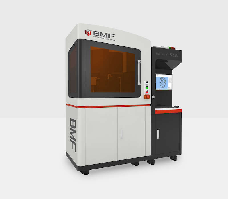
microArch S230
Ultra-high-resolution micro 3D printing for the finest features, tightest tolerances and near-final surface finishes — built on BMF’s Projection Micro Stereolithography (PµSL).
- 2µm XY optical resolution
- ±0.2µm XY positional accuracy
- Photopolymer resins and ceramics
Built for What Only 2µm Can Do
Finest Feature Resolution
2µm XY optical resolution produces micro-scale channels, walls and features that lower-resolution systems simply can’t — with parts that closely match the CAD model.
Exceptional Surface Quality
Surface roughness of 0.4–0.8µm Ra on top surfaces and 1.5–2.5µm Ra on side walls — ideal for optics, fluidics and biomedical applications.
Advanced Print Technology
A fast roller recoating system, stable light source and air-floated platform deliver the process control and repeatability that R&D and low-volume production demand.
What 2µm Resolution Makes Possible
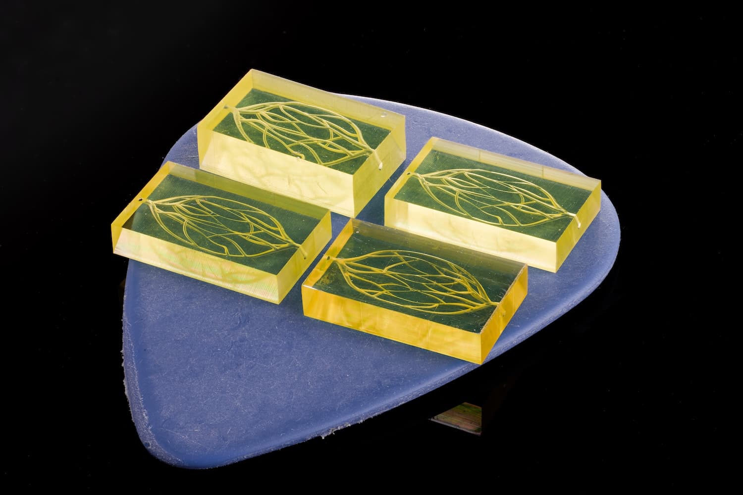
Blood Vessel Microfluidic Chip
Vascular channels just 43µm in diameter for research and device development.
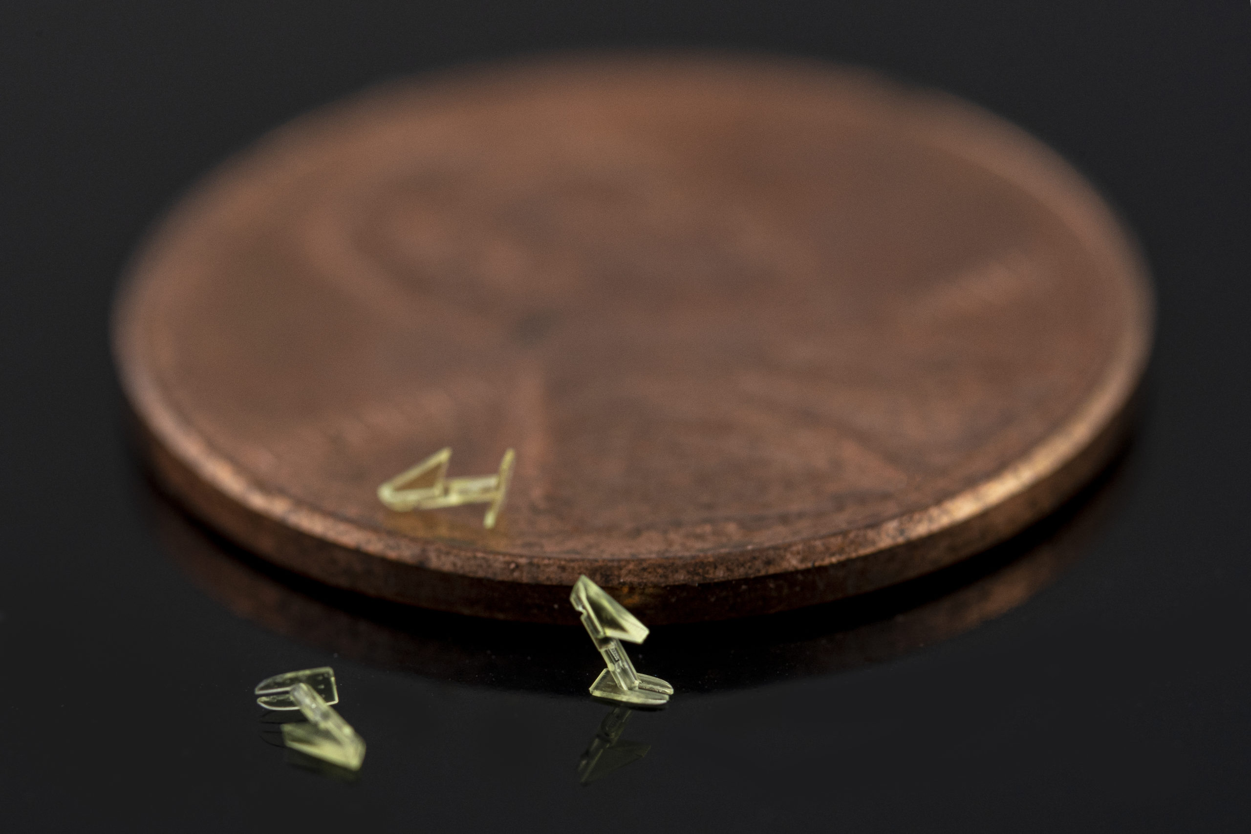
Glaucoma Stent
A sub-2mm implantable device with 110µm wall thickness and a 200µm internal channel — comparable to micro injection molding, at a fraction of the lead time.
See the S230 in Action
Resolution × Accuracy × Precision
Dimensional performance at the limits of additive manufacturing — 2µm optical resolution, ±0.2µm positional accuracy and light source stability for fine micro-scale geometry across materials.
Advanced Roller System
Spreads resin layers in seconds, for build speeds up to 5× faster than conventional recoating.
High-Viscosity Material Support
Processes higher-viscosity materials, including ceramic formulations for thermal or chemical resistance.
Air-Floated Platform
Isolates the build from mechanical vibration to hold sub-micron positional accuracy.
Light Source Stability
Consistent UV exposure from layer to layer and build to build for repeatable results.
Step-and-Repeat Process
A proprietary optical process pairs ultra-high resolution with a usable build area.
Real-Time Image Monitoring
Integrated auto-focus, exposure compensation and live monitoring let operators step in before defects spread.
Projection Micro Stereolithography
PµSL projects patterned UV light through a precision optical system to photopolymerize an entire resin layer at once. Combined with real-time exposure control and the air-floated platform, it achieves feature resolution and accuracy that conventional 3D printing and micro injection molding can’t match at equivalent lead times.
Print directly from STL — no tooling, no minimum order and no mold lead time.
Where the S230 Fits
Applications
- Medical devices and implantables
- Microfluidics and lab-on-chip
- Electronics and micro connectors
- Optics and fiber optics
- Ceramic components
- Micro mechatronics
Why It Matters
- Highest resolution in the microArch lineup
- Sub-micron positional accuracy
- Near-final surface finish straight off the printer
- Polymer and ceramic printing in one system
- Parts in days instead of waiting on micro molds
- Ideal for R&D and low-volume production
Specifications
Frequently Asked Questions
What makes the S230 different from other microArch printers?
The S230 is BMF’s 2µm system — the highest optical resolution in the lineup — with ±0.2µm positional accuracy. It’s designed for parts where the finest features and tightest tolerances matter most.
Can the S230 print ceramics?
Yes. Its high-viscosity material support allows ceramic formulations in addition to photosensitive resins, for parts that need thermal or chemical resistance.
What surface finish can I expect?
Top surfaces reach 0.4–0.8µm Ra and side walls 1.5–2.5µm Ra, which suits optical, fluidic and biomedical parts.
How does PµSL compare with micro injection molding?
PµSL prints directly from an STL file with no tooling, no minimum order and no mold lead time, while delivering molding-like feature resolution — making it well suited to prototyping and low-volume production.
How large is the build area?
The S230 builds parts up to 50 × 50 × 50 mm, using a step-and-repeat optical process to combine 2µm resolution with a usable build area.

